|
|
|
PDF IRF3205 Data sheet ( Hoja de datos )
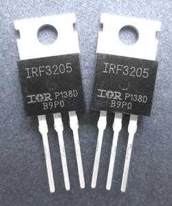
| Número de pieza | IRF3205 | |
| Descripción | N-Channel Trench Process Power MOSFET Transistor | |
| Fabricantes | Thinki Semiconductor | |
| Logotipo | ||
 1. 55V, 110A, HEXFET Power MOSFET Hay una vista previa y un enlace de descarga de IRF3205 (archivo pdf) en la parte inferior de esta página. Total 5 Páginas | ||
|
No Preview Available !
IRF3205
®
Pb Free Plating Product
IRF3205
Pb
N-Channel Trench Process Power MOSFET Transistor
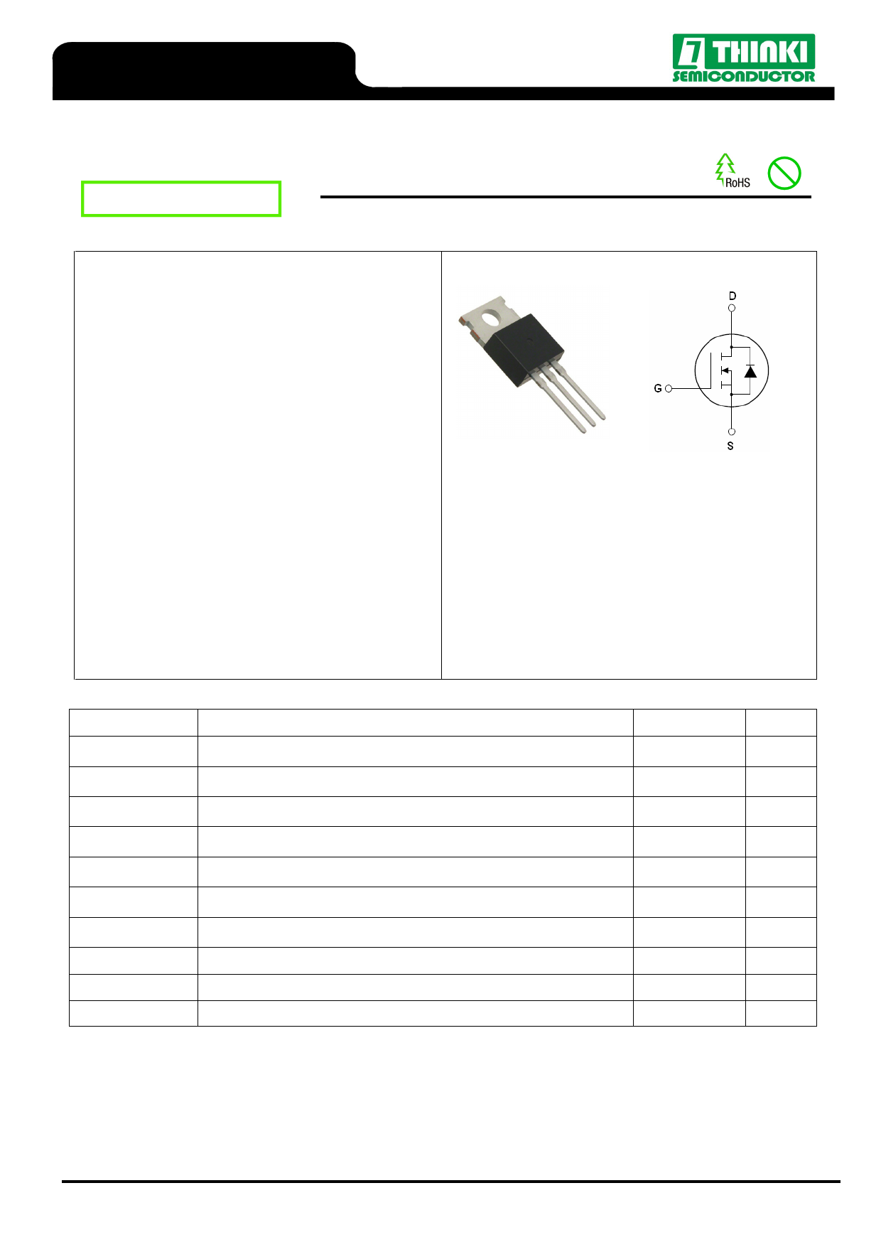
General Description
The IRF3205 is N-channel MOS Field Effect Transistor
designed for high current switching applications. Rugged
EAS capability and ultra low RDS(ON) is suitable for PWM,
load switching .
Features
● VDS=55V; ID=105A@ VGS=10V;
RDS(ON)<6.0mΩ @ VGS=10V
● Ultra Low On-Resistance
● High UIS and UIS 100% Test
Application
● Hard Switched and High Frequency Circuits
● Uninterruptible Power Supply
● Inverter Application
G DS
TO-220CB Top View
Schematic Diagram
VDS = 55 V
ID = 105 A
RDS(ON) = 5.0 mΩ
Table 1. Absolute Maximum Ratings (TA=25℃)
Symbol
Parameter
VDS Drain-Source Voltage (VGS=0V)
VGS Gate-Source Voltage (VDS=0V)
ID (DC)
ID (DC)
IDM (pluse)
Drain Current (DC) at Tc=25℃
Drain Current (DC) at Tc=100℃
Drain Current-Continuous@ Current-Pulsed (Note 1)
dv/dt
Peak Diode Recovery Voltage
PD Maximum Power Dissipation(Tc=25℃)
Derating Factor
EAS Single Pulse Avalanche Energy (Note 2)
TJ,TSTG
Operating Junction and Storage Temperature Range
Notes 1.Repetitive Rating: Pulse width limited by maximum junction temperature
2.EAS condition:TJ=25℃,VDD=40V,VBGB=10V,RG=25Ω
Value
55
±25
105
100
420
30
139
0.926
625
-55 To 175
Unit
V
V
A
A
A
V/ns
W
W/℃
mJ
℃
Rev.05
© 2013 Thinki Semiconductor Co.,Ltd.
Page 1/5
http://www.thinkisemi.com/
1 page 
IRF3205
®
Figure7. Capacitance vs Vds
7000
6000
Ciss
5000
4000
3000
2000
1000
Coss
Crss
0 0 5 10 15 20 25
VDS Drain-Source Voltage (V)
Figure9. BVDSS vs Junction Temperature
Figure8. Safe Operation Area
VDS Drain-Source Voltage (V)
Figure10. VGS(th) vs Junction Temperature
TJ-Junction Temperature(℃)
TJ-Junction Temperature(℃)
Figure11. Normalized Maximum Transient Thermal Impedance
Rev.05
© 2013 Thinki Semiconductor Co.,Ltd.
Page 5/5
http://www.thinkisemi.com/
5 Page | ||
| Páginas | Total 5 Páginas | |
| PDF Descargar | [ Datasheet IRF3205.PDF ] | |
Hoja de datos destacado
| Número de pieza | Descripción | Fabricantes |
| IRF320 | N-CHANNEL POWER MOSFETS | Samsung semiconductor |
| IRF320 | 2.8A and 3.3A/ 350V and 400V/ 1.8 and 2.5 Ohm/ N-Channel Power MOSFETs | Intersil Corporation |
| IRF320 | N-Channel Power MOSFETs/ 3.0 A/ 350-400 V | Fairchild Semiconductor |
| IRF320 | N-Channel MOSFET Transistor | Inchange Semiconductor |
| Número de pieza | Descripción | Fabricantes |
| SLA6805M | High Voltage 3 phase Motor Driver IC. |
Sanken |
| SDC1742 | 12- and 14-Bit Hybrid Synchro / Resolver-to-Digital Converters. |
Analog Devices |
|
DataSheet.es es una pagina web que funciona como un repositorio de manuales o hoja de datos de muchos de los productos más populares, |
| DataSheet.es | 2020 | Privacy Policy | Contacto | Buscar |