|
|
|
PDF SN74LS256 Data sheet ( Hoja de datos )
| Número de pieza | SN74LS256 | |
| Descripción | DUAL 4-BIT ADDRESSABLE LATCH | |
| Fabricantes | Motorola Semiconductors | |
| Logotipo | ||
Hay una vista previa y un enlace de descarga de SN74LS256 (archivo pdf) en la parte inferior de esta página. Total 6 Páginas | ||
|
No Preview Available !
DUAL 4-BIT
ADDRESSABLE LATCH
The SN54/74LS256 is a Dual 4-Bit Addressable Latch with common control
inputs; these include two Address inputs (A0, A1), an active LOW Enable input
(E) and an active LOW Clear input (CL). Each latch has a Data input (D) and
four outputs (Q0 – Q3).
When the Enable (E) is HIGH and the Clear input (CL) is LOW, all outputs
(Q0 – Q3) are LOW. Dual 4-channel demultiplexing occurs when the (CL) and
E are both LOW. When CL is HIGH and E is LOW, the selected output
(Q0 – Q3), determined by the Address inputs, follows D. When the E goes
HIGH, the contents of the latch are stored. When operating in the addressable
latch mode (E = LOW, CL = HIGH), changing more than one bit of the Address
(A0, A1) could impose a transient wrong address. Therefore, this should be
done only while in the memory mode (E= CL = HIGH).
• Serial-to-Parallel Capability
• Output From Each Storage Bit Available
• Random (Addressable) Data Entry
• Easily Expandable
• Active Low Common Clear
• Input Clamp Diodes Limit High Speed Termination Effects
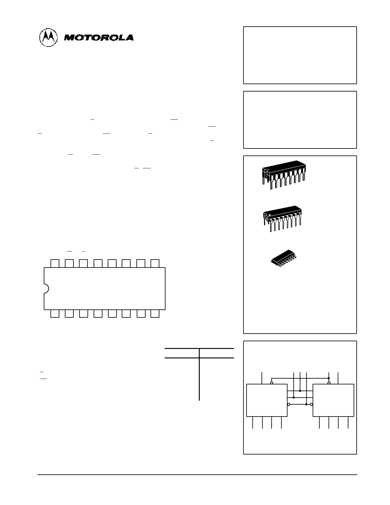
CONNECTION DIAGRAM DIP (TOP VIEW)
VCC CL E Db Q3b Q2b Q1b Q0b
16 15 14 13 12 11 10 9
NOTE:
The Flatpak version
has the same pinouts
(Connection Diagram) as
the Dual In-Line Package.
12
A0 A1
3 4 56 78
Da Q0a Q1a Q2a Q3a GND
PIN NAMES
LOADING (Note a)
HIGH
LOW
A0, A1
Da, Db
E
Address Inputs
Data Inputs
Enable Input (Active LOW)
0.5 U.L.
0.5 U.L.
1.0 U.L.
0.25 U.L.
0.25 U.L.
0.5 U.L.
CL Clear Input (Active LOW)
0.5 U.L.
0.25 U.L.
Q0a – Q3a,
Q0b – Q3b
Parallel Latch Outputs (Note b)
10 U.L. 5 (2.5) U.L.
NOTES:
a) 1 TTL Unit Load (U.L.) = 40 µA HIGH/1.6 mA LOW.
b) The Output LOW drive factor is 2.5 U.L. for Military (54) and 5 U.L. for Commercial
(74) Temperature Ranges.
SN54/74LS256
DUAL 4-BIT
ADDRESSABLE LATCH
LOW POWER SCHOTTKY
16
1
16
1
16
1
J SUFFIX
CERAMIC
CASE 620-09
N SUFFIX
PLASTIC
CASE 648-08
D SUFFIX
SOIC
CASE 751B-03
ORDERING INFORMATION
SN54LSXXXJ
SN74LSXXXN
SN74LSXXXD
Ceramic
Plastic
SOIC
LOGIC SYMBOL
3
2 1 15
14 13
Da E
A0
A1
CL
Q0a Q1a Q2a Q3a
A0 E Db
A1
CL
Q0b Q1b Q2b Q3b
4 56 7
9 10 11 12
VCC = PIN 16
GND = PIN 8
FAST AND LS TTL DATA
5-421
1 page 
Case 751B-03 D Suffix
16-Pin Plastic
SO-16
-A-
16 9
-B-
P 0.25 (0.010) M
BM
1
8 PL
8
G
-T-
D16 PL
0.25 (0.010) M T B S
AS
C
SEATING
PLANE
K
R X 45°
MF
J
Case 648-08 N Suffix
16-Pin Plastic
-A-
16 9
B
18
F
C
S
-T-
SEATING
PLANE
L
H
G
D 16 PL
K
0.25 (0.010) M T A M
J
M
Case 620-09 J Suffix
-A- 16-Pin Ceramic Dual In-Line
16 9
-B-
18
CL
-T-
SEATING
PLANE
F
E
G
D 16 PL
N
0.25 (0.010) M T A S
K
M
J 16 PL
0.25 (0.010) M T B S
NOTES:
1. DIMENSIONING AND TOLERANCING PER ANSI
Y14.5M, 1982.
2. CONTROLLING DIMENSION: MILLIMETER.
3. DIMENSION A AND B DO NOT INCLUDE MOLD
PROTRUSION.
4. MAXIMUM MOLD PROTRUSION 0.15 (0.006)
PER SIDE.
5. 751BĆ01 IS OBSOLETE, NEW STANDARD
751BĆ03.
DIM
A
B
C
D
F
G
J
K
M
P
R
MILLIMETERS
MIN MAX
9.80
10.00
3.80
4.00
1.35
1.75
0.35
0.49
0.40
1.25
1.27 BSC
0.19
0.25
0.10
0°Ă
0.25
7°Ă
5.80
6.20
0.25
0.50
INCHES
MIN MAX
0.386
0.393
0.150
0.157
0.054
0.068
0.014
0.019
0.016
0.049
0.050 BSC
0.008
0.009
0.004
0°Ă
0.009
7°Ă
0.229
0.244
0.010
0.019
NOTES:
1. DIMENSIONING AND TOLERANCING PER ANSI
Y14.5M, 1982.
2. CONTROLLING DIMENSION: INCH.
3. DIMENSION L" TO CENTER OF LEADS WHEN
FORMED PARALLEL.
4. DIMENSION B" DOES NOT INCLUDE MOLD
FLASH.
5. ROUNDED CORNERS OPTIONAL.
6. 648Ć01 THRU Ć07 OBSOLETE, NEW STANDARD
648Ć08.
DIM
A
B
C
D
F
G
H
J
K
L
M
S
MILLIMETERS
MIN MAX
18.80
19.55
6.35
6.85
3.69
4.44
0.39
0.53
1.02
1.77
2.54 BSC
1.27 BSC
0.21
0.38
2.80
3.30
7.50
0°
7.74
10°
0.51
1.01
INCHES
MIN MAX
0.740
0.770
0.250
0.270
0.145
0.175
0.015
0.021
0.040
0.070
0.100 BSC
0.050 BSC
0.008
0.015
0.110
0.130
0.295
0°
0.305
10°
0.020
0.040
NOTES:
1. DIMENSIONING AND TOLERANCING PER ANSI
Y14.5M, 1982.
2. CONTROLLING DIMENSION: INCH.
3. DIMENSION L TO CENTER OF LEAD WHEN
FORMED PARALLEL.
4. DIM F MAY NARROW TO 0.76 (0.030) WHERE
THE LEAD ENTERS THE CERAMIC BODY.
5. 620Ć01 THRU Ć08 OBSOLETE, NEW STANDARD
620Ć09.
DIM
A
B
C
D
E
F
G
J
K
L
M
N
MILLIMETERS
MIN MAX
19.05 19.55
6.10
7.36
Ċ 4.19
0.39
0.53
1.27 BSC
1.40
1.77
2.54 BSC
0.23
0.27
Ċ 5.08
7.62 BSC
0° 15°
0.39
0.88
INCHES
MIN MAX
0.750
0.770
0.240
0.290
Ċ 0.165
0.015
0.021
0.050 BSC
0.055
0.070
0.100 BSC
0.009
0.011
Ċ 0.200
0.300 BSC
0° 15°
0.015
0.035
FAST AND LS TTL DATA
5-425
5 Page | ||
| Páginas | Total 6 Páginas | |
| PDF Descargar | [ Datasheet SN74LS256.PDF ] | |
Hoja de datos destacado
| Número de pieza | Descripción | Fabricantes |
| SN74LS251 | Data Selectors/Multiplexers With 3-State Outputs | Texas Instruments |
| SN74LS251 | LOW POWER SCHOTTKY | ON Semiconductor |
| SN74LS251 | 8-INPUT MULTIPLEXER | Motorola Semiconductors |
| SN74LS253 | Dual 4-Line To 1-Line Data Selectors/Multiplexers With 3-State Outputs | Texas Instruments |
| Número de pieza | Descripción | Fabricantes |
| SLA6805M | High Voltage 3 phase Motor Driver IC. |
Sanken |
| SDC1742 | 12- and 14-Bit Hybrid Synchro / Resolver-to-Digital Converters. |
Analog Devices |
|
DataSheet.es es una pagina web que funciona como un repositorio de manuales o hoja de datos de muchos de los productos más populares, |
| DataSheet.es | 2020 | Privacy Policy | Contacto | Buscar |