|
|
PDF HT7333-7 Data sheet ( Hoja de datos )
| Número de pieza | HT7333-7 | |
| Descripción | 30V 250mA TinyPower LDO | |
| Fabricantes | Holtek Semiconductor | |
| Logotipo | ||
Hay una vista previa y un enlace de descarga de HT7333-7 (archivo pdf) en la parte inferior de esta página. Total 19 Páginas | ||
|
No Preview Available !
HT73xx-7
30V, 250mA TinyPowerTM LDO with Protections
Features
• Low power consumption
• Low voltage drop
• Low temperature coefficient
• High input voltage – up to 30V
• Output voltage accuracy: tolerance ±2%
• Over current protection
• Over temperature protection
• Chip enable/disable function
• Package types: 8-pin SOP-EP, SOT89-3 and
TO92-3
Applications
• Battery-powered equipment
• Communication equipment
• Audio/Video equipment
General Description
The HT73xx-7 is a low power high voltage series of
regulators implemented in CMOS technology which
has the advantages of low voltage drop and low
quiescent current. They allow input voltages as high
as 30V and are available with several fixed output
voltages ranging from 2.1V to 5.0V.
When the CE input is low, a fast discharge path pulls
the output voltage low via an internal pull-down
resistor. An internal over-current protection circuit
prevents the device from damage even if the output
is shorted to ground. An over-temperature protection
circuit ensures the device junction temperature will
not exceed a temperature of 150°C.
Selection Table
Part No.
HT7321-7
HT7323-7
HT7325-7
HT7327-7
HT7330-7
HT7333-7
HT7336-7
HT7340-7
HT7344-7
HT7350-7
Output Voltage
2.1V
2.3V
2.5V
2.7V
3.0V
3.3V
3.6V
4.0V
4.4V
5.0V
Note: "xx" stands for output voltages.
Packages
Markings
8SOP-EP
HT73xx-7 for the 8SOP-EP type.
TO92-3, SOT89-3 73xx-7 marking for the TO92-3, SOT89-3 types.
Rev. 1.00
1 April 15, 2016
1 page 
HT73xx-7
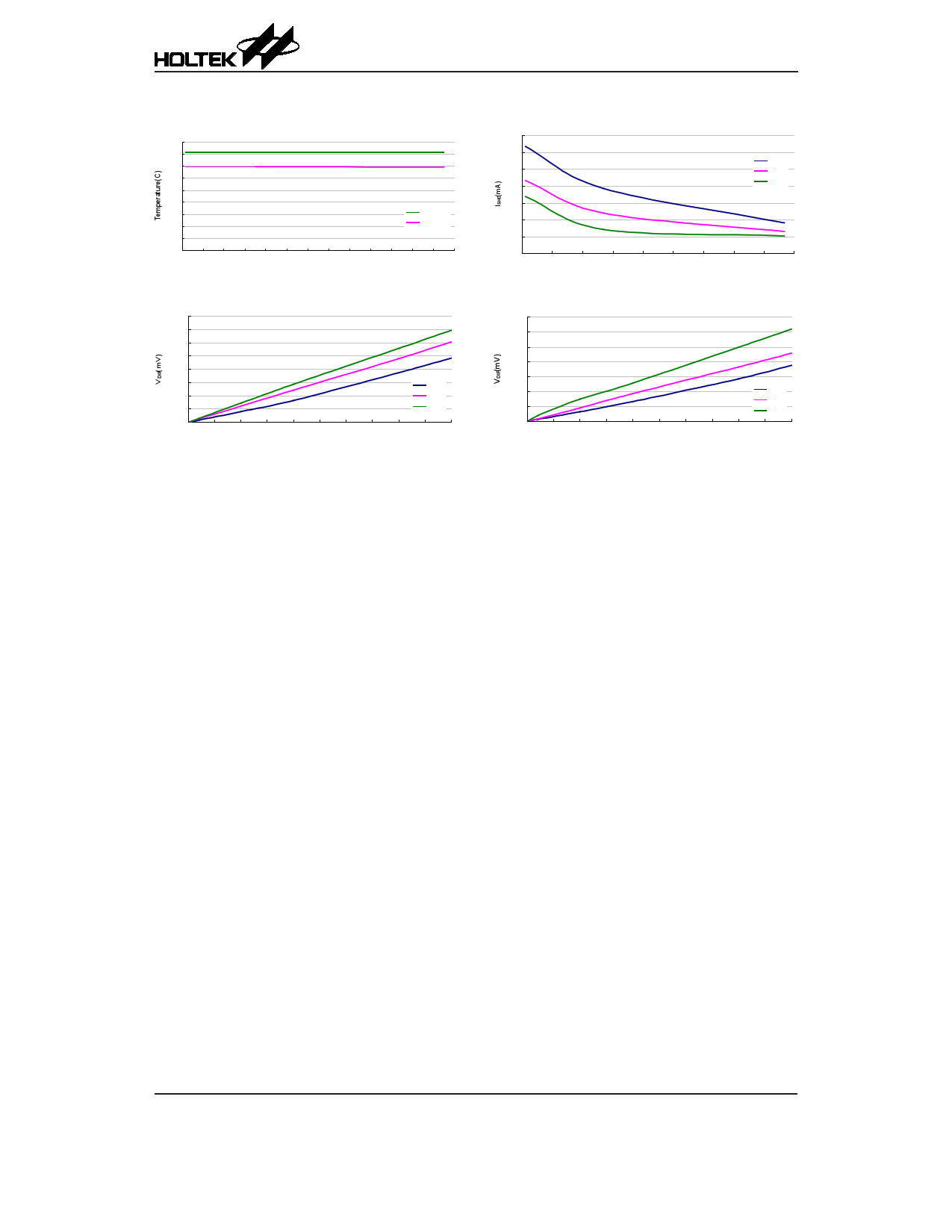
Test Condition: VIN=VOUT+2V, VCE=VIN, IOUT=10mA, CIN=10μF, COUT=10μF and Ta=25ºC, unless otherwise noted
180
160
140
120
100
80
60 TSHD(+)
40 THD(-)
20
0
5 7 9 11 13 15 17 19 21 23 25 27 29 31
VIN(V)
TSHD vs VIN
700
600
500
400
300
200
100
0
4
-40°C
25°C
85°C
7 10 13 16 19 22 25 28 31
VIN(V)
ISHD vs VIN
1600
1400
1200
1000
800
600
400
200
0
0
-40°C
25°C
85°C
25 50 75 100 125 150 175 200 225 250
IOUT(mA)
Dropout Voltage: HT7333-7
1400
1200
1000
800
600
400
200
0
0
-40°C
25°C
85°C
25 50 75 100 125 150 175 200 225 250
IOUT(mA)
Dropout Voltage: HT7350-7
Rev. 1.30
5 April 15, 2016
5 Page 
HT73xx-7
Application Information
When using the HT73xx-7 regulators, it is important
that the following application points are noted if
correct operation is to be achieved.
External Circuit
It is important that external capacitors are connected
to both the input and output pins. For the input pin
suitable bypass capacitors as shown in the application
circuits should be connected especially in situations
where a battery power source is used which may have
a higher impedance. For the output pin, a suitable
capacitor should also be connected especially in
situations where the load is of a transient nature, in
which case larger capacitor values should be selected
to limit any output transient voltages.
Thermal Considerations
The maximum power dissipation depends on the
thermal resistance of the package, the PCB layout,
the rate of the surrounding airflow and the difference
between the junction and ambient temperature. The
maximum power dissipation can be calculated using
the following formula:
PD(MAX) = (TJ(MAX) – Ta) / θJA
where TJ(MAX) is the maximum junction temperature,
Ta is the ambient temperature and θJA is the junction-
to-ambient thermal resistance of the IC package in
degrees per watt. The following table shows the θJA
values for various package types.
Package
SOT89-3
TO92-3
8SOP-EP
θJA value °C/W
200°C/W
200°C/W
125°C/W
For maximum operating rating conditions, the
maximum junction temperature is 150°C. However,
it is recommended that the maximum junction
temperature does not exceed 125°C during normal
operation to maintain an adequate margin for device
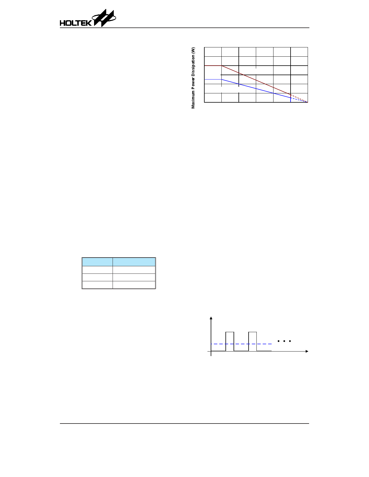
reliability. The derating curves of different packages
for maximum power dissipation are as follows:
1.0
0.8W
0.8
0.6 0.5W
8SOP-EP
0.4
SOT89-3, TO92-3
0.2
0
0 25 50 75 100
Ambient Temperature (oC)
125
150
Power Dissipation Calculation
In order to keep the device within its operating limits
and to maintain a regulated output voltage, the power
dissipation of the device, given by PD, must not
exceed the Maximum Power Dissipation, given by
PD(MAX). Therefore PD ≤ PD(MAX). From the diagram it
can be seen that almost all of this power is generated
across the pass transistor which is acting like a
variable resistor in series with the load to keep the
output voltage constant. This generated power which
will appear as heat, must never allow the device to
exceed its maximum junction temperature.
In practical applications the regulator may be called
upon to provide both steady state and transient
currents due to the transient nature of the load.
Although the device may be working well within its
limits with its steady state current, care must be taken
with transient loads which may cause the current to
rise close to its maximum current value. Care must
be taken with transient loads and currents as this will
result in device junction temperature rises which must
not exceed the maximum junction temperature. With
both steady state and transient currents, the important
current to consider is the average or more precisely
the RMS current which is the value of current that will
appear as heat generated in the device. The following
diagram shows how the average current relates to the
transient currents.
ILOAD
ILOAD(AVG)
Time
Rev. 1.30
11 April 15, 2016
11 Page | ||
| Páginas | Total 19 Páginas | |
| PDF Descargar | [ Datasheet HT7333-7.PDF ] | |
Hoja de datos destacado
| Número de pieza | Descripción | Fabricantes |
| HT7333-2 | 30V 250mA TinyPower LDO | Holtek Semiconductor |
| HT7333-7 | 30V 250mA TinyPower LDO | Holtek Semiconductor |
| Número de pieza | Descripción | Fabricantes |
| SLA6805M | High Voltage 3 phase Motor Driver IC. |
Sanken |
| SDC1742 | 12- and 14-Bit Hybrid Synchro / Resolver-to-Digital Converters. |
Analog Devices |
|
DataSheet.es es una pagina web que funciona como un repositorio de manuales o hoja de datos de muchos de los productos más populares, |
| DataSheet.es | 2020 | Privacy Policy | Contacto | Buscar |
