|
|
PDF LT8302 Data sheet ( Hoja de datos )
| Número de pieza | LT8302 | |
| Descripción | Micropower No-Opto Isolated Flyback Converter | |
| Fabricantes | Linear Technology | |
| Logotipo |  |
|
Hay una vista previa y un enlace de descarga de LT8302 (archivo pdf) en la parte inferior de esta página. Total 26 Páginas | ||
|
No Preview Available !
Features
n 2.8V to 42V Input Voltage Range
n 3.6A, 65V Internal DMOS Power Switch
n Low Quiescent Current:
106µA in Sleep Mode
380µA in Active Mode
n Quasi-Resonant Boundary Mode Operation at
Heavy Load
n Low Ripple Burst Mode® Operation at Light Load
n Minimum Load < 0.5% (Typ) of Full Output
n No Transformer Third Winding or Opto-Isolator
Required for Output Voltage Regulation
n Accurate EN/UVLO Threshold and Hysteresis
n Internal Compensation and Soft-Start
n Temperature Compensation for Output Diode
n Output Short-Circuit Protection
n Thermally Enhanced 8-Lead SO Package
Applications
n Isolated Automotive, Industrial, Medical Power
Supplies
n Isolated Auxiliary/Housekeeping Power Supplies
LT8302
42VIN Micropower No-Opto
Isolated Flyback Converter
with 65V/3.6A Switch
Description
The LT®8302 is a monolithic micropower isolated flyback
converter. By sampling the isolated output voltage directly
from the primary-side flyback waveform, the part requires
no third winding or opto-isolator for regulation. The output
voltage is programmed with two external resistors and a
third optional temperature compensation resistor. Bound-
ary mode operation provides a small magnetic solution with
excellent load regulation. Low ripple Burst Mode operation
maintains high efficiency at light load while minimizing the
output voltage ripple. A 3.6A, 65V DMOS power switch
is integrated along with all the high voltage circuitry and
control logic into a thermally enhanced 8-lead SO package.
The LT8302 operates from an input voltage range of 2.8V
to 42V and delivers up to 18W of isolated output power.
The high level of integration and the use of boundary
and low ripple burst modes result in a simple to use, low
component count, and high efficiency application solution
for isolated power delivery.
L, LT, LTC, LTM, Linear Technology, the Linear logo and Burst Mode are registered trademarks
of Linear Technology Corporation. All other trademarks are the property of their respective
owners. Protected by U.S. Patents, including 5438499, 7463497, 7471522.
Typical Application
2.8V to 32VIN/5VOUT Isolated Flyback Converter
VIN
2.8V TO 32V
10µF
VIN
EN/UVLO SW
LT8302
GND RFB
INTVCC
1µF
RREF
TC
470pF
3:1
•
9µH
39Ω •
1µH
VOUT+
5V
220µF
VOUT–
154k
115k 10k
10mA TO 1.1A (VIN = 5V)
10mA TO 2.0A (VIN = 12V)
10mA TO 2.9A (VIN = 24V)
8302 TA01a
For more information www.linear.com/LT8302
Efficiency vs Load Current
90
FRONT PAGE APPLICATION
85
80
75
70
65
VIN = 5V
VIN = 12V
VIN = 24V
60
0 0.5 1.0 1.5 2.0 2.5 3.0
LOAD CURRENT (A)
8302 TA01b
8302fb
1
1 page 
LT8302
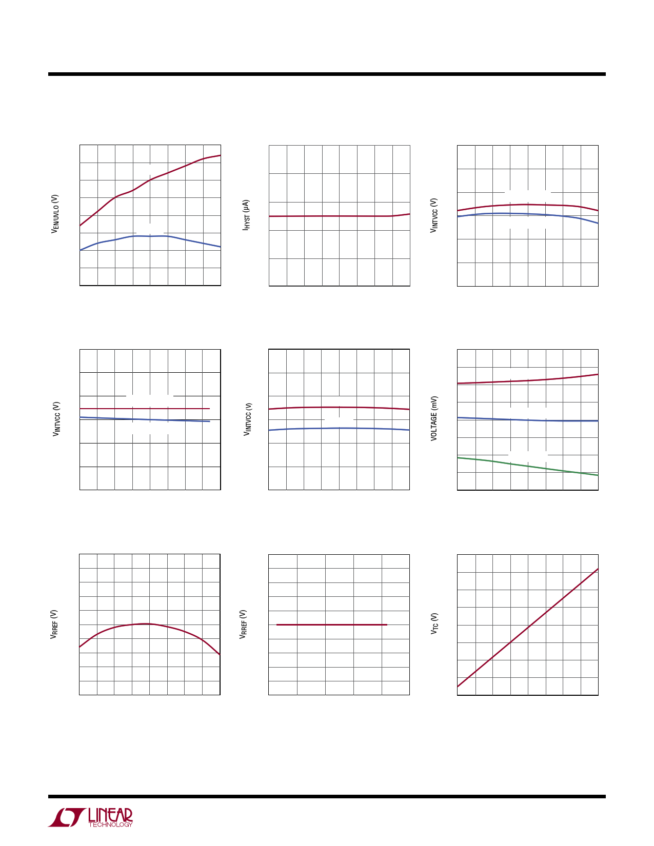
Typical Performance Characteristics TA = 25°C, unless otherwise noted.
EN/UVLO Enable Threshold
1.240
1.235
1.230
RISING
1.225
1.220
1.215
FALLING
1.210
1.205
1.200
–50 –25
0 25 50 75 100 125 150
TEMPERATURE (°C)
8302 G10
INTVCC Voltage vs VIN
3.10
3.05
3.00 IINTVCC = 0mA
2.95
IINTVCC = 10mA
2.90
2.85
2.80
5
10 15 20 25 30 35 40 45
VIN (V)
8302 G13
RREF Regulation Voltage
1.010
1.008
1.006
1.004
1.002
1.000
0.998
0.996
0.994
0.992
0.990
–50 –25
0 25 50 75 100 125 150
TEMPERATURE (°C)
8302 G16
EN/UVLO Hysteresis Current
5
4
3
2
1
0
–50 –25
0 25 50 75 100 125 150
TEMPERATURE (°C)
8302 G11
INTVCC UVLO Threshold
2.8
2.7
2.6 RISING
2.5 FALLING
2.4
2.3
2.2
–50 –25
0 25 50 75 100 125 150
TEMPERATURE (°C)
8302 G14
RREF Line Regulation
1.010
1.008
1.006
1.004
1.002
1.000
0.998
0.996
0.994
0.992
0.990
0
10 20 30
VIN (V)
40 50
8302 G17
INTVCC Voltage vs Temperature
3.10
3.05
3.00
2.95
2.90
IINTVCC = 0mA
IINTVCC = 10mA
2.85
2.80
–50 –25
0 25 50 75 100 125 150
TEMPERATURE (°C)
8302 G12
(RFB-VIN) Voltage
40
30 IRFB = 125µA
20
10
0 IRFB = 100µA
–10
–20 IRFB = 75µA
–30
–40
–50 –25
0 25 50 75 100 125 150
TEMPERATURE (°C)
8302 G15
TC Pin Voltage
1.5
1.4
1.3
1.2
1.1
1.0
0.9
0.8
0.7
–50 –25
0 25 50 75 100 125 150
TEMPERATURE (°C)
8302 G18
For more information www.linear.com/LT8302
8302fb
5
5 Page 
LT8302
Applications Information
Output Voltage
The RFB and RREF resistors as depicted in the Block Diagram
are external resistors used to program the output voltage.
The LT8302 operates similar to traditional current mode
switchers, except in the use of a unique flyback pulse
sense circuit and a sample-and-hold error amplifier, which
sample and therefore regulate the isolated output voltage
from the flyback pulse.
Operation is as follows: when the power switch M1 turns
off, the SW pin voltage rises above the VIN supply. The
amplitude of the flyback pulse, i.e., the difference between
the SW pin voltage and VIN supply, is given as:
VFLBK = (VOUT + VF + ISEC • ESR) • NPS
VF = Output diode forward voltage
ISEC = Transformer secondary current
ESR = Total impedance of secondary circuit
NPS = Transformer effective primary-to-secondary
turns ratio
The flyback voltage is then converted to a current, IRFB,
by the RFB resistor and the flyback pulse sense circuit
(M2 and M3). This current, IRFB, also flows through the
RREF resistor to generate a ground-referred voltage. The
resulting voltage feeds to the inverting input of the sample-
and-hold error amplifier. Since the sample-and-hold error
amplifier samples the voltage when the secondary current
is zero, the (ISEC • ESR) term in the VFLBK equation can be
assumed to be zero.
The internal reference voltage, VREF, 1.00V, feeds to the
noninverting input of the sample-and-hold error ampli-
fier. The relatively high gain in the overall loop causes the
voltage at the RREF pin to be nearly equal to the internal
reference voltage VREF. The resulting relationship between
VFLBK and VREF can be expressed as:
⎛
⎝⎜
VFLBK
RFB
⎞
⎠⎟
• RREF
=
VREF
or
VFLBK
=
VREF
•
⎛
⎝⎜
RFB
RREF
⎞
⎠⎟
VREF = Internal reference voltage 1.00V
Combination with the previous VFLBK equation yields an
equation for VOUT, in terms of the RFB and RREF resistors,
transformer turns ratio, and diode forward voltage:
VOUT
=
VREF
•
⎛
⎝⎜
RFB
RREF
⎞
⎠⎟
•
⎛
⎝⎜
1
NPS
⎞
⎠⎟
–
VF
Output Temperature Compensation
The first term in the VOUT equation does not have tempera-
ture dependence, but the output diode forward voltage, VF,
has a significantnegativetemperaturecoefficient (–1mV/°C
to –2mV/°C). Such a negative temperature coefficient pro-
duces approximately 200mV to 300mV voltage variation
on the output voltage across temperature.
For higher voltage outputs, such as 12V and 24V, the
output diode temperature coefficient has a negligible ef-
fect on the output voltage regulation. For lower voltage
outputs, such as 3.3V and 5V, however, the output diode
temperature coefficient does count for an extra 2% to 5%
output voltage regulation.
The LT8302 junction temperature usually tracks the output
diode junction temperature tothefirst order. Tocompensate
the negative temperature coefficient of the output diode,
a resistor, RTC, connected between the TC and RREF pins
generates a proportional-to-absolute-temperature (PTAT)
current. The PTAT current is zero at 25°C, flows into the
RREF pin at hot temperature, and flows out of the RREF pin
at cold temperature. With the RTC resistor in place, the
output voltage equation is revised as follows:
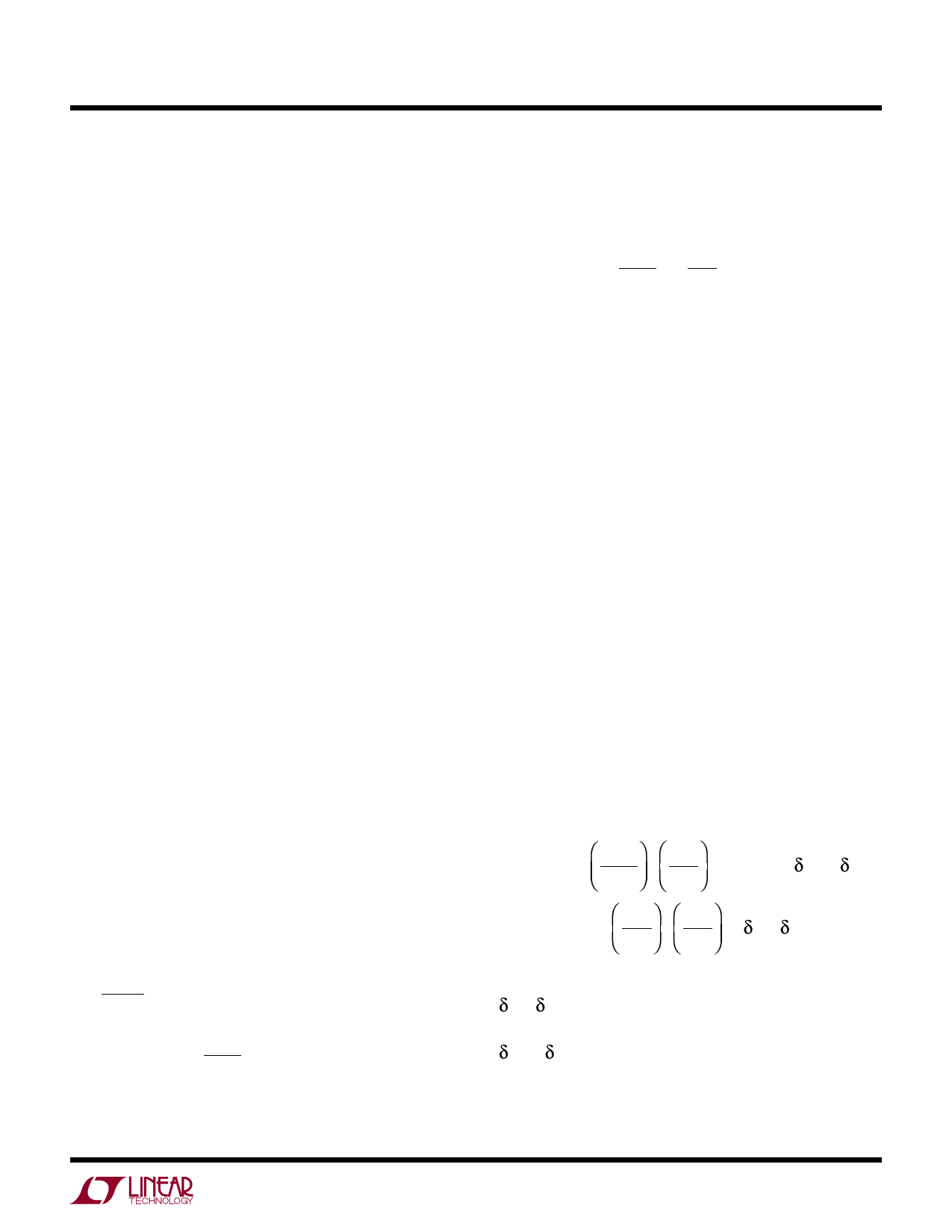
( ) ( )VOUT = VREF •
RFB
RREF
•
1
NPS
– VF TO –
VTC / T •
(T –TO)•
RFB
RTC
•
1
NPS
– ( VF /
T ) • ( T – TO)
TO=Room temperature 25°C
( VF / T) = Oteumtppuetradtiuordeecfooerfwfiacriednvtoltage
( VTC / T) = 3.35mV/°C
For more information www.linear.com/LT8302
8302fb
11
11 Page | ||
| Páginas | Total 26 Páginas | |
| PDF Descargar | [ Datasheet LT8302.PDF ] | |
Hoja de datos destacado
| Número de pieza | Descripción | Fabricantes |
| LT8300 | 100VIN Micropower Isolated Flyback Converter | Linear Technology |
| LT8301 | Micropower No-Opto Isolated Flyback Converter | Linear Technology |
| LT8302 | Micropower No-Opto Isolated Flyback Converter | Linear Technology |
| LT8303 | Micropower Isolated Flyback Converter | Linear |
| Número de pieza | Descripción | Fabricantes |
| SLA6805M | High Voltage 3 phase Motor Driver IC. |
Sanken |
| SDC1742 | 12- and 14-Bit Hybrid Synchro / Resolver-to-Digital Converters. |
Analog Devices |
|
DataSheet.es es una pagina web que funciona como un repositorio de manuales o hoja de datos de muchos de los productos más populares, |
| DataSheet.es | 2020 | Privacy Policy | Contacto | Buscar |
