|
|
PDF RT9745A Data sheet ( Hoja de datos )
| Número de pieza | RT9745A | |
| Descripción | Low Resistance Load Switch | |
| Fabricantes | Richtek | |
| Logotipo |  |
|
Hay una vista previa y un enlace de descarga de RT9745A (archivo pdf) en la parte inferior de esta página. Total 16 Páginas | ||
|
No Preview Available !
®
RT9745A
Dual Channel, Low Resistance Load Switch
General Description
The RT9745A is a small, low RON, dual channel load switch
with EN controlled pin. The product contains two N-
MOSFETs that can operate between an input voltage range
of 0.8V to 5.5V. Also, it supports a maximum continuous
current of 6A each channel. Each switch is independently
controlled by EN pins (EN1 and EN2), which can directly
interface with low-voltage control signals.
The RT9745A is available in the WDFN-14TL 3x2 package
with exposed pad for high power and heat dissipation.
Ordering Information
RT9745A
Package Type
QW : WDFN-14TL 3x2 (W-Type)
Note :
Lead Plating System
G : Green (Halogen Free and Pb Free)
Richtek products are :
RoHS compliant and compatible with the current require-
ments of IPC/JEDEC J-STD-020.
Suitable for use in SnPb or Pb-free soldering processes.
Marking Information
0P : Product Code
0PW
W : Date Code
Features
Integrated Dual Channel Load Switch
Input Voltage Range : 0.8V to 5.5V
Low RON Resistance
RON = 27mΩ at VIN = 5V (VDD = 5V)
RON = 27mΩ at VIN = 3.6V (VDD = 5V)
RON = 27mΩ at VIN = 1.8V (VDD = 5V)
6A Maximum Continuous Switch Current Per
Channel
Low Quiescent Current
75μA (Both Channels)
55μA (Single Channel)
Low Control Input Threshold Enables Use of 1.4V/
1.8V/2.5V/3.3V Logics
Configurable Rise Time
Quick Output Discharge (QOD)
Adaptive Discharge Current
14T-Lead WDFN Package with Thermal Pad
Applications
UltrabookTM
Notebooks/Netbooks
Tablet PC
Consumer Electronics
Set-Top Boxes/Residential Gateways
Telecom Systems
Solid State Drives (SSD)
Simplified Application Circuit
CIN1
Dual Power
Supply
or
Dual DC/DC
Converter
Enable
Enable
CIN2
VIN1
VOUT1
RT9745A
EN1
VDD
EN2
VIN2
SS1
SS2
VOUT2
GND
COUT1
VOUT1
RL1
CSS1
CSS2
COUT2
VOUT2
RL2
Copyright ©2014 Richtek Technology Corporation. All rights reserved.
DS9745A-00 August 2014
is a registered trademark of Richtek Technology Corporation.
www.richtek.com
1
1 page 
RT9745A
Parameter
Symbol
Test Conditions
Min Typ Max Unit
VIN1,2 = 5V -- -- 8
VIN1,2 Off-State Supply Current
(Per Channel)
IIN(VIN, OFF)
VEN1,2 = GND,
VOUT1,2 = 0V
VIN1,2 = 3.3V
VIN1,2 = 1.8V
--
--
--
--
3
2
A
VIN1,2 = 0.8V -- -- 1
Resistance Characteristics
VIN = 5V
-- 27 30
VIN = 3.3V
-- 27 30
ON-State Resistance
RON
IOUT = 200mA,
VDD = 5V
VIN = 1.8V
VIN = 1.5V
--
--
27
27
30
30
m
VIN = 1.2V
-- 27 30
VIN = 0.8V
-- 27 30
Output Pull-down Resistance RPD
VEN = 0V, VIN = 5V, IOUT = 15mA
-- 220 300
Note 1. Stresses beyond those listed “Absolute Maximum Ratings” may cause permanent damage to the device. These are
stress ratings only, and functional operation of the device at these or any other conditions beyond those indicated in
the operational sections of the specifications is not implied. Exposure to absolute maximum rating conditions may
affect device reliability.
Note 2. θJA is measured at TA = 25°C on a high effective thermal conductivity four-layer test board per JEDEC 51-7. θJC is
measured at the exposed pad of the package.
Note 3. Devices are ESD sensitive. Handling precaution is recommended.
Note 4. The device is not guaranteed to function outside its operating conditions.
Copyright ©2014 Richtek Technology Corporation. All rights reserved.
DS9745A-00 August 2014
is a registered trademark of Richtek Technology Corporation.
www.richtek.com
5
5 Page 
RT9745A
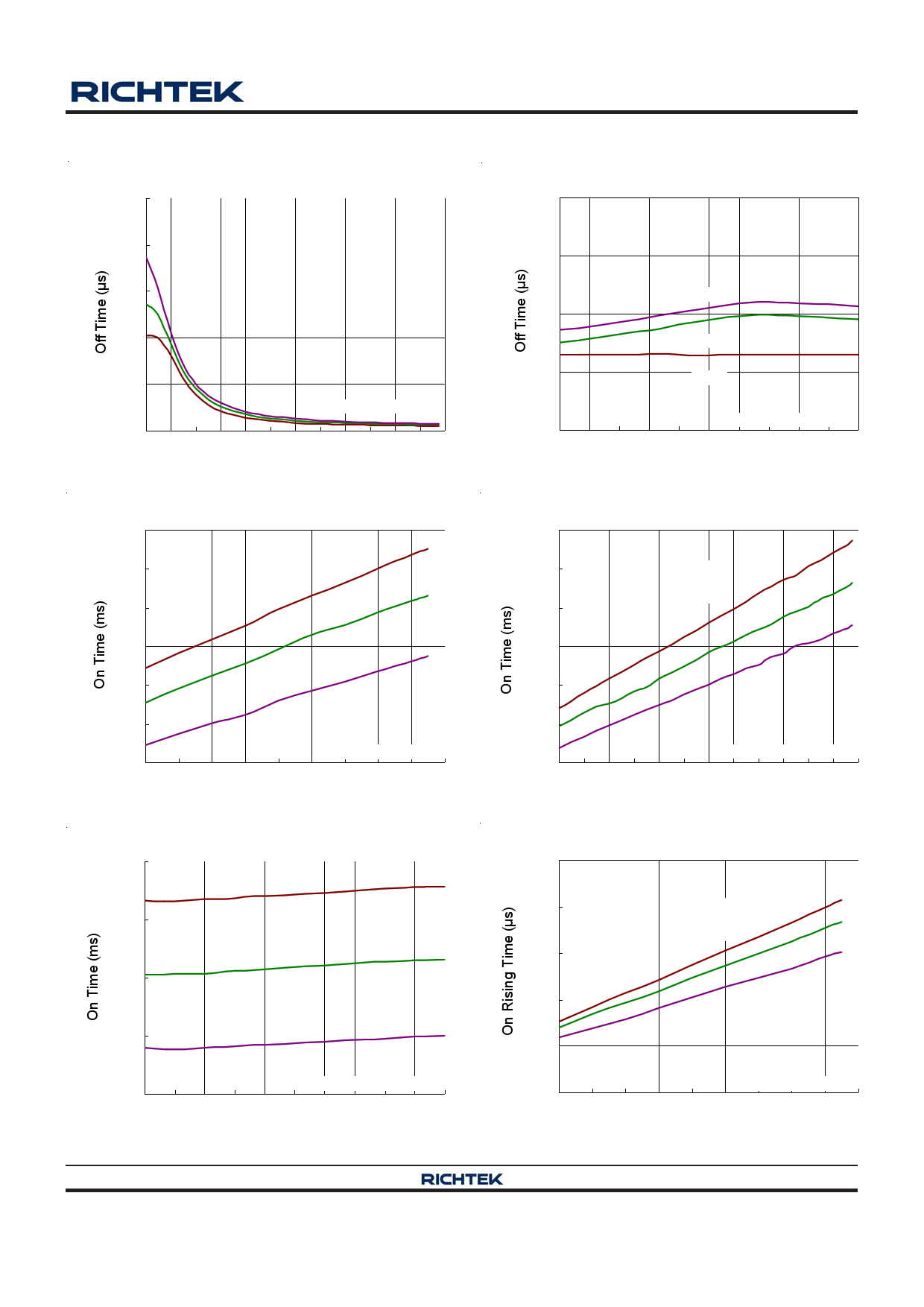
Off Time vs. Input Voltage
150
120
85°C
90 25°C
−40°C
60
30
VDD = 5.5V, CSS = 1nF
0
0.8 1.2 1.6 2 2.4 2.8 3.2 3.6 4 4.4 4.8 5.2 5.6
Input Voltage (V)
On Time vs. Input Voltage
1000
900 −40°C
800
700
25°C
600
500 85°C
VDD = 2.5V, CSS = 1nF
400
0.8 1 1.2 1.4 1.6 1.8 2 2.2 2.4 2.6
Input Voltage (V)
On Time vs. VDD
1000
−40°C
900
800 25°C
700
85°C
VIN = 2.5V, CSS = 1nF
600
2.5 2.8 3.1 3.4 3.7 4 4.3 4.6 4.9 5.2 5.5
VDD (V)
Copyright ©2014 Richtek Technology Corporation. All rights reserved.
DS9745A-00 August 2014
Off Time vs. VDD
20
15
85°C
10
25°C
5 −40°C
VIN = 2.5V, CSS = 1nF
0
2.5 2.8 3.1 3.4 3.7 4 4.3 4.6 4.9 5.2 5.5
VDD (V)
On Time vs. Input Voltage
1600
1400
1200
−40°C
25°C
85°C
1000
800
600
VDD = 5.5V, CSS = 1nF
400
0.8 1.2 1.6 2 2.4 2.8 3.2 3.6 4 4.4 4.8 5.2 5.6
Input Voltage (V)
On Rising Time vs. Input Voltage
1000
800 −40°C
25°C
85°C
600
400
200
VDD = 2.5V, CSS = 1nF
0
0.8 1 1.2 1.4 1.6 1.8 2 2.2 2.4 2.6
Input Voltage (V)
is a registered trademark of Richtek Technology Corporation.
www.richtek.com
11
11 Page | ||
| Páginas | Total 16 Páginas | |
| PDF Descargar | [ Datasheet RT9745A.PDF ] | |
Hoja de datos destacado
| Número de pieza | Descripción | Fabricantes |
| RT9745A | Low Resistance Load Switch | Richtek |
| Número de pieza | Descripción | Fabricantes |
| SLA6805M | High Voltage 3 phase Motor Driver IC. |
Sanken |
| SDC1742 | 12- and 14-Bit Hybrid Synchro / Resolver-to-Digital Converters. |
Analog Devices |
|
DataSheet.es es una pagina web que funciona como un repositorio de manuales o hoja de datos de muchos de los productos más populares, |
| DataSheet.es | 2020 | Privacy Policy | Contacto | Buscar |
