|
|
|
PDF AD6673 Data sheet ( Hoja de datos )
| Número de pieza | AD6673 | |
| Descripción | Dual IF Receiver | |
| Fabricantes | Analog Devices | |
| Logotipo | ||
Hay una vista previa y un enlace de descarga de AD6673 (archivo pdf) en la parte inferior de esta página. Total 30 Páginas | ||
|
No Preview Available !
Data Sheet
80 MHz Bandwidth, Dual IF Receiver
AD6673
FEATURES
JESD204B Subclass 0 or Subclass 1 coded serial digital outputs
Signal-to-noise ratio (SNR) = 71.9 dBFS at 185 MHz AIN and
250 MSPS with NSR set to 33%
Spurious-free dynamic range (SFDR) = 88 dBc at 185 MHz
AIN and 250 MSPS
Total power consumption: 707 mW at 250 MSPS
1.8 V supply voltages
Integer 1-to-8 input clock divider
Sample rates of up to 250 MSPS
IF sampling frequencies of up to 400 MHz
Internal analog-to-digital converter (ADC) voltage reference
Flexible analog input range
1.4 V p-p to 2.0 V p-p (1.75 V p-p nominal)
ADC clock duty cycle stabilizer (DCS)
95 dB channel isolation/crosstalk
Serial port control
Energy saving power-down modes
APPLICATIONS
Communications
Diversity radio and smart antenna (MIMO) systems
Multimode digital receivers (3G)
TD-SCDMA, WiMAX, WCDMA,
CDMA2000, GSM, EDGE, LTE
I/Q demodulation systems
General-purpose software radios
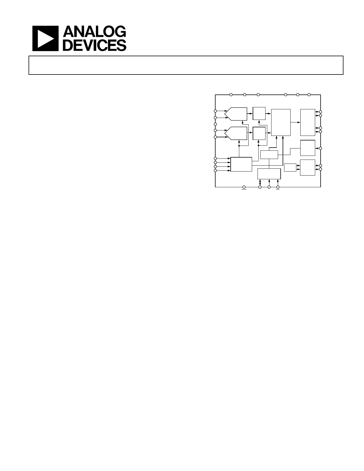
VIN+A
VIN–A
VCM
VIN+B
VIN–B
SYSREF±
SYNCINB±
CLK±
RFCLK
FUNCTIONAL BLOCK DIAGRAM
AVDD DRVDD DVDD
AGND DGND DRGND
PIPELINE
11-BIT ADC
PIPELINE
11-BIT ADC
NSR
NSR
JESD-204B
INTERFACE
HIGH
SPEED
SERIALIZERS
AD6673
CML, TX
OUTPUTS
SERDOUT0±
SERDOUT1±
CLOCK
GENERATION
CONTROL
REGISTERS
CMOS
DIGITAL
INPUT
CMOS
DIGITAL
INPUT/OUTPUT
FAST
DETECT
CMOS
DIGITAL
OUTPUT
PDWN
FDA
FDB
RST
SDIO SCLK CS
Figure 1.
PRODUCT HIGHLIGHTS
1. The configurable JESD204B output block with an integrated
phase-locked loop (PLL) to support up to 5 Gbps per lane
with up to two lanes.
2. IF receiver includes two, 11-bit, 250 MSPS ADCs with
programmable noise shaping requantizer (NSR) function that
allows for improved SNR within a reduced bandwidth of 22%
or 33% of the sample rate.
3. Support for an optional RF clock input to ease system board
design.
4. Proprietary differential input maintains excellent SNR
performance for input frequencies of up to 400 MHz.
5. An on-chip integer, 1-to-8 input clock divider and SYNC
input allows synchronization of multiple devices.
6. Operation from a single 1.8 V power supply.
7. Standard serial port interface (SPI) that supports various
product features and functions, such as controlling the clock
DCS, power-down, test modes, voltage reference mode,
overrange fast detection, and serial output configuration.
This product may be protected by one or more U.S. or international patents.
Rev. C
Document Feedback
Information furnished by Analog Devices is believed to be accurate and reliable. However, no
responsibilityisassumedbyAnalogDevices for itsuse,nor foranyinfringementsofpatentsor other
rights of third parties that may result from its use. Specifications subject to change without notice. No
license is granted by implication or otherwise under any patent or patent rights of Analog Devices.
Trademarksandregisteredtrademarksarethepropertyoftheirrespectiveowners.
One Technology Way, P.O. Box 9106, Norwood, MA 02062-9106, U.S.A.
Tel: 781.329.4700 ©2012–2015 Analog Devices, Inc. All rights reserved.
Technical Support
www.analog.com
1 page 
Data Sheet
AD6673
SPECIFICATIONS
ADC DC SPECIFICATIONS
AVDD = 1.8 V, DRVDD = 1.8 V, DVDD = 1.8 V, maximum sample rate for speed grade, VIN = −1.0 dBFS differential input, 1.75 V p-p
full-scale input range, DCS enabled, link parameters used are M = 2 and L = 2, unless otherwise noted.
Table 1.
Parameter
RESOLUTION
ACCURACY
No Missing Codes
Offset Error
Gain Error
Differential Nonlinearity (DNL)
Integral Nonlinearity (INL)1
MATCHING CHARACTERISTIC
Offset Error
Gain Error
TEMPERATURE DRIFT
Offset Error
Gain Error
INPUT REFERRED NOISE
VREF = 1.0 V
ANALOG INPUT
Input Span
Input Capacitance2
Input Resistance3
Input Common-Mode Voltage
POWER SUPPLIES
Supply Voltage
AVDD
DRVDD
DVDD
Supply Current
IAVDD
IDRVDD + IDVDD
NSR Disabled
NSR Enabled, 22% Mode
NSR Enabled, 33% Mode
POWER CONSUMPTION
Sine Wave Input
NSR Disabled
NSR Enabled, 22% Mode
NSR Enabled, 33% Mode
Standby Power4
Power-Down Power
Temperature
Full
Full
Full
Full
Full
25°C
Full
25°C
Full
Full
Full
Full
25°C
Full
Full
Full
Full
Full
Full
Full
Full
Full
Full
Full
Full
Full
Full
Full
Full
Full
Full
Min Typ Max
11
Guaranteed
−16 +16
−6 +2.5
±0.6
±0.25
±0.7
±0.3
−15 +15
−2 +3
±2
±50
0.32
1.75
2.5
20
0.9
1.7 1.8 1.9
1.7 1.8 1.9
1.7 1.8 1.9
254 282
139 150
187
211
707
794
837
334
9
Unit
Bits
mV
%FSR
LSB
LSB
LSB
LSB
mV
%FSR
ppm/°C
ppm/°C
LSB rms
V p-p
pF
kΩ
V
V
V
V
mA
mA
mA
mA
mA
mW
mW
mW
mW
mW
1 Measured with a low input frequency, full-scale sine wave.
2 Input capacitance refers to the effective capacitance between one differential input pin and its complement.
3 Input resistance refers to the effective resistance between one differential input pin and its complement.
4 Standby power is measured with a dc input and the CLK± pin active.
Rev. C | Page 5 of 45
5 Page 
Data Sheet
ABSOLUTE MAXIMUM RATINGS
Table 6.
Parameter
ELECTRICAL
AVDD to AGND
DRVDD to AGND
DVDD to DGND
VIN+A/VIN+B, VIN−A/VIN−B to AGND
CLK+, CLK− to AGND
RFCLK to AGND
VCM to AGND
CS, PDWN to AGND
SCLK to AGND
SDIO to AGND
RST to DGND
FDA, FDB to DGND
SERDOUT0+, SERDOUT0−,
SERDOUT1+, SERDOUT1− to AGND
SYNCINB+, SYNCINB− to DGND
SYSREF+, SYSREF− to AGND
ENVIRONMENTAL
Operating Temperature Range
(Ambient)
Maximum Junction Temperature
Under Bias
Storage Temperature Range
(Ambient)
Rating
−0.3 V to +2.0 V
−0.3 V to +2.0 V
−0.3 V to +2.0 V
−0.3 V to AVDD + 0.2 V
−0.3 V to AVDD + 0.2 V
−0.3 V to AVDD + 0.2 V
−0.3 V to AVDD + 0.2 V
−0.3 V to AVDD + 0.3 V
−0.3 V to AVDD + 0.3 V
−0.3 V to AVDD + 0.3 V
−0.3 V to DVDD + 0.3 V
−0.3 V to DVDD + 0.3 V
−0.3 V to DRVDD + 0.3 V
−0.3 V to DVDD + 0.3 V
−0.3 V to AVDD + 0.3 V
−40°C to +85°C
150°C
−65°C to +125°C
Stresses at or above those listed under Absolute Maximum
Ratings may cause permanent damage to the product. This is a
stress rating only; functional operation of the product at these
or any other conditions above those indicated in the operational
section of this specification is not implied. Operation beyond
the maximum operating conditions for extended periods may
affect product reliability.
AD6673
THERMAL CHARACTERISTICS
The exposed paddle must be soldered to the ground plane for
the LFCSP package. This increases the reliability of the solder
joints, maximizing the thermal capability of the package.
Table 7. Thermal Resistance
Package Type
Airflow
Velocity
(m/sec)
48-Lead LFCSP
7 mm × 7 mm
(CP-48-13)
0
1.0
2.5
θJA1, 2
25
22
20
θJC1, 3
2
θJB1, 4
14
1 Per JEDEC 51-7, plus JEDEC 25-5 2S2P test board.
2 Per JEDEC JESD51-2 (still air) or JEDEC JESD51-6 (moving air).
3 Per MIL-STD-883, Method 1012.1.
4 Per JEDEC JESD51-8 (still air).
Unit
°C/W
°C/W
°C/W
Typical θJA is specified for a 4-layer printed circuit board (PCB)
with a solid ground plane. As shown in Table 7, airflow increases
heat dissipation, which reduces θJA. In addition, metal in direct
contact with the package leads from metal traces, through holes,
ground, and power planes reduces the θJA.
ESD CAUTION
Rev. C | Page 11 of 45
11 Page | ||
| Páginas | Total 30 Páginas | |
| PDF Descargar | [ Datasheet AD6673.PDF ] | |
Hoja de datos destacado
| Número de pieza | Descripción | Fabricantes |
| AD667 | Microprocessor-Compatible 12-Bit D/A Converter | Analog Devices |
| AD6672 | IF Receiver | Analog Devices |
| AD6673 | Dual IF Receiver | Analog Devices |
| AD6674 | 385 MHz BW IF Diversity Receiver | Analog Devices |
| Número de pieza | Descripción | Fabricantes |
| SLA6805M | High Voltage 3 phase Motor Driver IC. |
Sanken |
| SDC1742 | 12- and 14-Bit Hybrid Synchro / Resolver-to-Digital Converters. |
Analog Devices |
|
DataSheet.es es una pagina web que funciona como un repositorio de manuales o hoja de datos de muchos de los productos más populares, |
| DataSheet.es | 2020 | Privacy Policy | Contacto | Buscar |