|
|
PDF PI6LC48S04 Data sheet ( Hoja de datos )
| Número de pieza | PI6LC48S04 | |
| Descripción | HiFlex Serial Interface Clock | |
| Fabricantes | Pericom Semiconductor | |
| Logotipo | ||
Hay una vista previa y un enlace de descarga de PI6LC48S04 (archivo pdf) en la parte inferior de esta página. Total 11 Páginas | ||
|
No Preview Available !
PI6LC48S04
HiFlex Serial Interface Clock
Features
ÎÎSelectable 250MHz, 156.25MHz, 125MHz or 100MHz output
clock synthesized from a 25MHz fundamental mode crystal
ÎÎFour differential clock outputs (two LVDS and two low power
HCSL outputs)
ÎÎCrystal interface designed for 25MHz, parallel resonant
crystal
ÎÎRMS phase jitter @ 156.25MHz, using a 25MHz crystal
(1MHz - 20MHz): 0.21ps (typical)
ÎÎRMS phase jitter @ 156.25MHz, using a 25MHz crystal
(12kHz - 20MHz): 0.32ps (typical)
ÎÎPower supply noise rejection PSNR: -50dB (typical)
ÎÎLVCMOS interface levels for the frequency select input
ÎÎFull 3.3V or 2.5V supply voltage
ÎÎLead-free (RoHS 6) packaging
ÎÎ-40°C to 85°C ambient operating temperature
Description
The PI6LC48S04 is a 4-output clock synthesizer designed for se-
rial reference clock applications. The device generates four cop-
ies of a selectable 250MHz, 156.25MHz, 125MHz or 100MHz
clock signal with 0.34ps phase jitter performance. The four
outputs are organized in two banks of two LVDS and two low
power HCSL ouputs.The device supports 3.3V and 2.5V voltage
supplies and is packaged in a small 32-lead TQFN package.
Function Table
Inputs
F_SEL [1]
F_SEL [0]
0 (default)
0
1
1
0 (default)
1
0
1
Note: F_SEL[1:0] are asynchronous controls.
Output Frequency
with fXTAL = 25MHz
156.25MHz
125MHz
100MHz
250MHz
Block Diagram
Pin Configuration
XTAL_IN
XTAL_OUT
REF_CLK
REF_SEL
BYPASS
F_SEL[0:1]
nOEA
nOEB
VSWING_CTRL
OSC 0
Pulldown
1
Pulldown
Pulldown
Pulldown
Pulldown
Pulldown
2
PFD VCO
&
LPF
: 25
1
:N
0
QA0+
QA0-
LVDS
QA1+
QA1-
LVDS
QB0+
QB0-
HCSL
QB1+
QB1-
HSCL
VDD
nc
VDDA
nc
GND
REF_CLK
nOEA
VDD
32 31 30 29 28 27 26 25
1 24
2 23
3 22
4 21
5 20
6 19
7 18
8 17
9 10 11 12 13 14 15 16
VSWING_CTRL
GND
QA0-
QA0+
VDDOA
QA1-
QA1+
GND
15-0128
1
PI6LC48S04 RevA
10/12/15
1 page 
PI6LC48S04
HiFlex Serial Interface Clock
Maximum Ratings
Note:
SInuppuptlsy..V...o..l.t..a..g..e.,..V...D..D..,.V...D..D..A.,..V..D..D..O..x.......-..0....5..V....t..o...V...D..D..+... 40..65VV
Storage Temperature, TSTG..................... -65oC to 150oC
Inputs (Referenced to GND)...........-0.5 to VDD+0.5V
Clock Output (Referenced to GND).............-0.5 to 2V
Latch up............................................................... .200mA
NOTE: Stresses beyond those listed under Absolute Maximum
Ratings may cause permanent damage to the device. These
ratings are stress specifications only. Functional operation of
the product at these conditions or any conditions beyond those
listed in the DC Characteristics or AC Characteristics is not
implied. Exposure to absolute maximum rating conditions for
extended periods may affect product reliability.
ESD Protection (Input)..................2000 V min (HBM)
DC Electrical Characteristics
Power Supply DC Characteristics (VDD = VDDOA = VDDOB = 3.3V±5% or 2.5V±5%, TA = -40°C to 85°C)
Symbol
VDD
VDDA
VDDOA&B
IDDA
IDD
IDDOA&B
Parameter
Core Supply Voltage
Output Supply Voltage
Output Supply Voltage
Analog Supply Current
Power Supply Current
Output Supply Current
Test Condition
Min.
3.135
2.375
VDD – 0.30
VDD – 0.30
3.135
2.375
Typ.
3.3
2.5
3.3
2.5
3.3
2.5
Max.
3.465
2.625
VDD
VDD
3.465
2.625
30
25
72
Units
V
V
V
V
V
V
mA
mA
mA
15-0128
5
PI6LC48S04 RevA
10/12/15
5 Page 
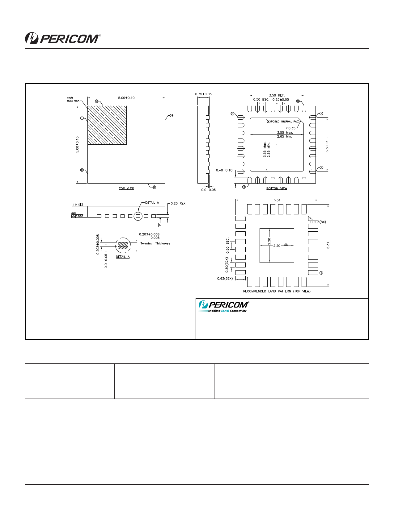
Packaging Mechanical:
PI6LC48S04
HiFlex Serial Interface Clock
Notes:
1. All dimensions are in mm. Angles in degrees.
2. Coplanarity applies to the exposed pad as well as the terminals.
3. Refer JEDEC MO-220
4. Recommended land pattern is for reference only.
5. Thermal pad soldering area (mesh stencile design is recommended)
11-0147
Ordering Information
DESCRIPTION: 32-contact, Thin Quad Flat No-Lead (TQFN)
PACKAGE CODE: ZH32
DOCUMENT CONTROL #: PD-2070
DATE: 06/30/11
REVISION: B
Ordering Code
PI6LC48S04ZHIE
PI6LC48S04ZHIEX
Package Code
ZH
ZH
Package Type
Pb-free & Green, 32-pin TQFN
Pb-free & Green, 32-pin TQFN, Tape & Reel
Notes:
1. Thermal characteristics can be found on the company web site at www.pericom.com/packaging/
2. “E” denotes Pb-free and Green
3. Adding an “X” at the end of the ordering code denotes tape and Reel packaging
15-0128
11
PI6LC48S04 RevA
10/12/15
11 Page | ||
| Páginas | Total 11 Páginas | |
| PDF Descargar | [ Datasheet PI6LC48S04.PDF ] | |
Hoja de datos destacado
| Número de pieza | Descripción | Fabricantes |
| PI6LC48S04 | HiFlex Serial Interface Clock | Pericom Semiconductor |
| Número de pieza | Descripción | Fabricantes |
| SLA6805M | High Voltage 3 phase Motor Driver IC. |
Sanken |
| SDC1742 | 12- and 14-Bit Hybrid Synchro / Resolver-to-Digital Converters. |
Analog Devices |
|
DataSheet.es es una pagina web que funciona como un repositorio de manuales o hoja de datos de muchos de los productos más populares, |
| DataSheet.es | 2020 | Privacy Policy | Contacto | Buscar |
