|
|
|
PDF PI6LC48C21 Data sheet ( Hoja de datos )
| Número de pieza | PI6LC48C21 | |
| Descripción | Single Output LVCMOS Clock Generator | |
| Fabricantes | Pericom Semiconductor | |
| Logotipo | ||
Hay una vista previa y un enlace de descarga de PI6LC48C21 (archivo pdf) en la parte inferior de esta página. Total 6 Páginas | ||
|
No Preview Available !
Features
ÎÎSingle LVCMOS output
ÎÎSupports 125MHz or 130MHz output frequencies
ÎÎRMS phase jitter @ 125MHz, using a 25MHz crystal
(1.875MHz – 20MHz): 0.15ps (typical)
ÎÎRMS phase jitter @ 125MHz, using a 25MHz crystal
(12kHz – 20MHz): 0.33ps (typical)
ÎÎFull 3.3V or 2.5V supply modes
ÎÎIndustrial ambient operating temperature
ÎÎAvailable in lead-free package: 8-TSSOP
Applications
ÎÎNetworking systems
PI6LC48C21
Single Output LVCMOS Clock Generator
Description
The PI6LC48C21 is a single LVCMOS output synthesizer opti-
mized to generate Ethernet reference clock frequencies and is a
member of Pericom’s HiFlex family of high performance clock
solutions. Using a 25MHz crystal, It can generate 125MHz with
very low phase jitter.
It is ideal for Ethernet interface in all kind of systems.
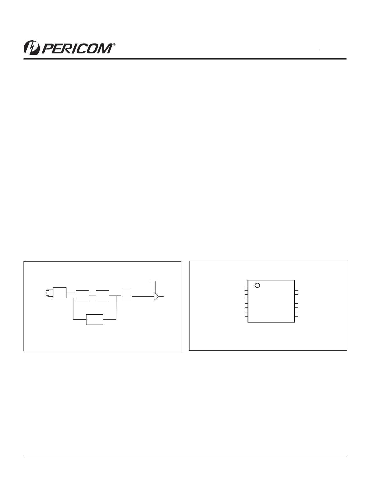
Block Diagram
Pin Configuration
XTAL_IN
XTAL_OUT
OSC
PFD VCO
/25
OE
/5 CLK
VDDA
OE
XTAL_OUT
XTAL_IN
1
2
3
4
8 VDD
7 CLK
6 GND
5 NC
15-0105
1 www.pericom.com
PI6LC48C21
Rev. B
08/04/15
1 page 
PI6LC48C21
Single Output LVCMOS Clock Generator
Crystal Input Interface
The clock generator has been characterized with 18pF parallel resonant crystals. The capacitor values shown in the figure below
were determined using a 25MHz, 18pF parallel resonant crystal and were chosen to minimize the ppm error.
LVCMOS to XTAL Interface
The XTAL_IN input can accept a single-ended LVCMOS signal through an AC coupling capacitor. A general interface diagram
is shown in the figure below. The XTAL_OUT pin can be left floating. The input edge rate can be as slow as 10ns. For LVCMOS
signals, it is recommended that the amplitude be reduced from full swing to half swing in order to prevent signal interference with
the power rail and to reduce noise. This configuration requires that the output impedance of the driver (Ro) plus the series resis-
tance (Rs) equals the transmission line impedance. In addition, matched termination at the crystal input will attenuate the signal in
half. This can be done in one of the two ways. First, R1 and R2 in parallel should equal the transmission line empedance. For most
50Ω applications, R1 and R2 can be 100Ω. This can also be accomplished by removing R1 and making R2 50Ω. By overdriving the
crystal oscillator, the device will be functional, but note, the device performance is quaranteed by using a quartz crystal.
VDD
Ro
Rs
Zo = Ro + Rs
50Ω
VDD
R1
0.1µF
XTAL_IN
R2
XTAL_OUT
15-0105
5 www.pericom.com
PI6LC48C21
Rev. B
08/04/15
5 Page | ||
| Páginas | Total 6 Páginas | |
| PDF Descargar | [ Datasheet PI6LC48C21.PDF ] | |
Hoja de datos destacado
| Número de pieza | Descripción | Fabricantes |
| PI6LC48C21 | Single Output LVCMOS Clock Generator | Pericom Semiconductor |
| Número de pieza | Descripción | Fabricantes |
| SLA6805M | High Voltage 3 phase Motor Driver IC. |
Sanken |
| SDC1742 | 12- and 14-Bit Hybrid Synchro / Resolver-to-Digital Converters. |
Analog Devices |
|
DataSheet.es es una pagina web que funciona como un repositorio de manuales o hoja de datos de muchos de los productos más populares, |
| DataSheet.es | 2020 | Privacy Policy | Contacto | Buscar |